Automated Optical Inspection Step 8. PCB Plating Step 11.
Metal Core Pcb Vs Standard Circuit Boards Differences In Pcb Type
Design Review and Engineering Questions Step 3.

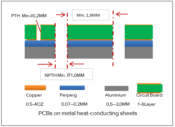
. Laminating the PCB Layers Step 9. We offer a full range of printed circuit board capabilities to fit all of your PCB needsCurrently we accept 5 PCB file formats gerber file pcb pcbdoc cam or brd file format for PCB fabrication. These design rules specify you must have a minimal isolation or spacing of 08mm 16mil between the copper elements of a typical carbon finger contacts.
The ESP32 family includes the chips ESP32-D0WDQ6 and ESP32-D0WD ESP32-D2WD ESP32-S0WD and the system in package SiP ESP32-PICO-D4At its heart theres a dual-core or single-core Tensilica Xtensa LX6. Created by Espressif Systems ESP32 is a low-cost low-power system on a chip SoC series with Wi-Fi dual-mode Bluetooth capabilities. Etch the Inner Layers or Core to Remove Copper Step 6.
Printing the PCB Design. Designing the PCB Step 2. Printing the Copper for the Interior Layer Step 5.
With advanced carbon PCB manufacturing capability our mininum values can be smaller but with longer lead time. Layer Alignment Step 7.

A Guide To Metal Core Pcbs By Pcbgogo Maker Portal

Metal Core Pcbs Pcb Prototype The Easy Way Pcbway

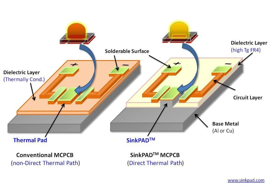
Metal Core Pcb Design Mc Pcb Design Expert With Complete Design Guide
The Basics Of Metal Core Pcb Design And Manufacturing Nwes Blog
The Basics Of Metal Core Pcb Design And Manufacturing Nwes Blog
King Credie Printed Circuit Board Pcb Manufacturing Online Quote
Metal Core Pcb Design And Manufacturing Guidelines
Metal Core Pcb Design Guidelines Flexible Factory For Led A Tech
0 comments
Post a Comment